




China’s Huawei touts chip design breakthrough in bid to defy U.S. sanctions
The Gist
Huawei Technologies Co., Ltd. said it has developed a new chip design framework aimed at “1.4nm-class transistors” and a 55% increase in transistor density, a claim the company presented May 25 at a tech conference in Shanghai as it seeks to keep advancing despite U.S. sanctions that have restricted its access to leading-edge semiconductor tools and technology.
Huawei Technologies Co., Ltd. said it has developed a new chip design framework aimed at “1.4nm-class transistors” and a 55% increase in transistor density, a claim the company presented May 25 at a tech conference in Shanghai as it seeks to keep advancing despite U.S. sanctions that have restricted its access to leading-edge semiconductor tools and technology [1]. The announcement, delivered by He Tingbo, president of Huawei’s semiconductor business, positioned the company’s latest work as a roadmap for pushing performance and miniaturization further even as global chipmaking has become increasingly shaped by geopolitics and export controls [1].
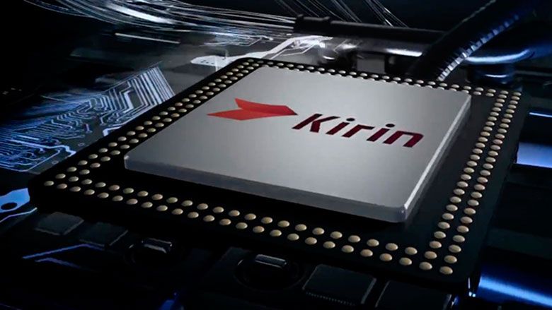
At the center of Huawei’s pitch was a design approach He Tingbo said the company calls “LogicFolding,” which he described as intended for future Kirin chips, Huawei’s flagship smartphone and device processors that have become a symbol of the company’s effort to rebuild high-end capabilities under restrictions [2]. NBC News reported that Huawei framed the concept as part of a broader attempt to keep improving chip performance through architectural and design innovations, rather than relying solely on the most advanced manufacturing access that U.S. policy has sought to limit [2]. He Tingbo’s use of the term “LogicFolding” underscored Huawei’s emphasis on design-side breakthroughs as a way to keep pace with the industry’s shrinking transistor dimensions and rising performance demands [2].
Huawei also introduced what NBC News described as a new principle called the “Tau Scaling Law,” which it said focuses on cutting chip performance, signaling an effort to articulate a new framework for how performance gains could be achieved as conventional scaling becomes harder and more expensive [2]. The company’s decision to brand a scaling principle reflects how chipmakers and designers are increasingly searching for new rules of thumb beyond traditional Moore’s Law-style expectations, particularly as the industry approaches physical and economic limits in transistor shrinking [2]. NBC News cited Huawei’s presentation of the “Tau Scaling Law” as part of the company’s broader message that it can still chart a path to cutting-edge chips through new design methodologies [2].
In its Shanghai conference remarks, Huawei said it had achieved a breakthrough that could allow it to make cutting-edge chips within five years, according to NBC News, a timeline that would be closely watched by competitors, suppliers and policymakers given the role advanced semiconductors play in smartphones, data centers and artificial intelligence systems [2]. Tom’s Hardware separately reported that Huawei’s framework targets 1.4nm-class transistors and a 55% increase in transistor density, a technical claim that, if realized, would represent a significant leap in packing more computing capability into the same area [1]. The company’s emphasis on density gains aligns with the industry’s ongoing drive to increase performance per watt and overall throughput by fitting more transistors onto a chip, even as manufacturing becomes more complex [1].
The announcements matter because they illustrate how Huawei is trying to reassert itself in high-end chip development by leaning on design innovation and long-term roadmaps, even as U.S. sanctions have aimed to curb China’s access to the most advanced semiconductor technologies [2]. By publicly laying out a path toward 1.4nm-class targets and naming new design principles, Huawei is signaling to the market—and to policymakers—that it intends to keep pushing toward the frontier of chip performance on a multi-year horizon [1][2]. Huawei’s choice to unveil these claims at a Shanghai tech conference on May 25 also highlights the role of domestic industry events as platforms for Chinese firms to showcase progress and rally local ecosystems around ambitious technology goals [1][2].
Huawei’s next test will be whether “LogicFolding” and the “Tau Scaling Law” translate from conference-stage concepts into measurable improvements in future Kirin chips, which He Tingbo said are the intended beneficiaries of the new design approach [2].
Sources (2)
Huawei claims sanctions-busting breakthrough with 1.4nm-class chips by 2031, claims 55% higher transistor density — firm claims new LogicFolding chip architecture can bypass EUV restrictions, introduces 'Tau Scaling Law' to replace Moore's Law
tomshardware.com
China’s Huawei touts chip design breakthrough in bid to defy U.S. sanctions
nbcnews.com
Published May 25, 2026
Synthesized from 2 sources